| CPC G02F 1/134309 (2013.01) [G02F 1/133345 (2013.01); G02F 1/136286 (2013.01)] | 20 Claims |
|
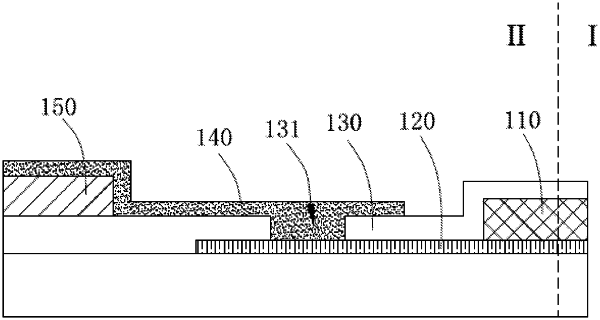
1. A display substrate, comprising a display region and a peripheral region surrounding the display region, wherein the display substrate comprises:
a common electrode line extending in a first direction on a base substrate, wherein the common electrode line is arranged at both the display region and the peripheral region;
a first conductive pattern arranged at the peripheral region and electrically connected to the common electrode line;
an insulation layer covering the first conductive pattern and the common electrode line, wherein a via-hole is formed in the insulation layer, and an orthogonal projection of the via-hole onto the base substrate does not overlap an orthogonal projection of the common electrode line onto the base substrate; and
a second conductive pattern arranged at the peripheral region and at a side of the insulation layer distal to the first conductive pattern, wherein the second conductive pattern is electrically connected to the first conductive pattern through the via-hole.
|