| CPC G02F 1/13306 (2013.01) [G02F 1/13454 (2013.01); G02F 1/13458 (2013.01); G02F 1/134309 (2013.01); G02F 1/136286 (2013.01); G09G 3/36 (2013.01); G09G 3/3614 (2013.01); G02F 2201/40 (2013.01); G09G 2310/0286 (2013.01); G09G 2310/08 (2013.01)] | 15 Claims |

|
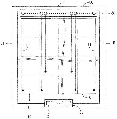
1. A liquid crystal display device including a panel substrate provided with a display region including a plurality of pixel electrodes, the liquid crystal display device comprising:
a plurality of pixel transistors that is provided in a region outside the display region and corresponds to the plurality of pixel electrodes in a one-to-one manner;
a plurality of pixel wiring lines configured to respectively connect the plurality of pixel electrodes to the plurality of pixel transistors;
an input pad group provided on the panel substrate and to which a drive signal group for driving the plurality of pixel transistors is input; and
a drive circuit configured to drive the plurality of pixel transistors based on the drive signal group,
wherein, in a region on the panel substrate, the plurality of pixel transistors is provided only in a first region other than a region between the input pad group and the display region,
in the region on the panel substrate, the drive circuit is provided in a second region other than the region between the input pad group and the display region such that the plurality of pixel transistors is disposed in a region between the drive circuit and the display region,
the drive circuit includes a decoding circuit including a plurality of output units,
the plurality of output units outputs, as a plurality of timing signals, a plurality of decoding signals that becomes active sequentially, and
capturing of a plurality of data signals included in the drive signal group is performed based on the plurality of timing signals.
|