| CPC G02B 6/428 (2013.01) [G02B 6/4214 (2013.01); G02B 6/4253 (2013.01); G02B 6/43 (2013.01); H01L 21/561 (2013.01); H01L 21/565 (2013.01); H01L 21/6835 (2013.01); H01L 23/3128 (2013.01); H01L 23/5386 (2013.01); H01L 24/24 (2013.01); H01L 24/82 (2013.01); H01L 24/96 (2013.01); H01L 25/18 (2013.01); H01L 25/50 (2013.01); H05K 1/0274 (2013.01); H05K 1/181 (2013.01); H01L 21/568 (2013.01); H01L 2221/68359 (2013.01); H01L 2221/68372 (2013.01); H01L 2221/68381 (2013.01); H01L 2224/215 (2013.01); H01L 2224/24225 (2013.01); H01L 2224/821 (2013.01); H01L 2224/82005 (2013.01); H01L 2224/95001 (2013.01); H01L 2924/12042 (2013.01); H01L 2924/12043 (2013.01); H05K 2201/10121 (2013.01); H05K 2201/10151 (2013.01); H05K 2201/2054 (2013.01)] | 20 Claims |
|
1. A package structure, comprising:
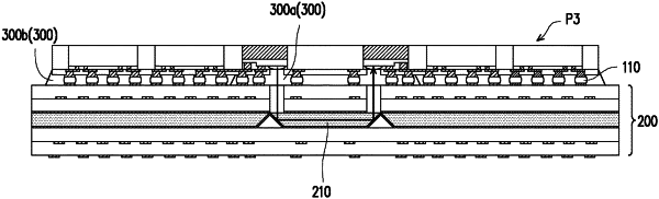
a circuit board comprising an optical waveguide;
a fanout package disposed over the circuit board, the fanout package comprising photoelectric integrated circuit dies, an insulating encapsulant laterally encapsulating the photoelectric integrated circuit dies, a redistribution circuit layer covering the photoelectric integrated circuit dies and the insulating encapsulant, and the photoelectric integrated circuit dies communicating with each other through the optical waveguide of the circuit board, wherein the redistribution circuit layer comprises a first optical window and a second optical window, the first optical window is between a first end of the optical waveguide and the photoelectric integrated circuit dies, and the second optical window is between a second end of the optical waveguide and the photoelectric integrated circuit dies.
|