| CPC G02B 6/34 (2013.01) [G02B 27/0081 (2013.01)] | 17 Claims |
|
1. A diffractive optical waveguide for optical pupil expansion, comprising:
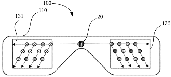
a waveguide substrate comprising a coupling-in region and a coupling-out region, wherein the coupling-out region includes a first coupling-out region and a second coupling-out region, and the first coupling-out region and the second coupling-out region are respectively used for corresponding to a left eye and a right eye of human eyes;
a coupling-in grating disposed on or in the waveguide substrate and located in the coupling-in region and configured to couple input light into the waveguide substrate to cause the light to propagate within the waveguide substrate through total reflection, wherein a first diffractive light obtained by the input light diffracted by the coupling-in grating is totally reflected in the waveguide substrate and directed to the first coupling-out region, and a second diffractive light obtained by the input light diffracted by the coupling-in grating is totally reflected in the waveguide substrate and directed to the second coupling-out region;
a coupling-out grating comprising a first coupling-out grating disposed on or in the waveguide substrate and located in the first coupling-out region and a second coupling-out grating disposed on or in the waveguide substrate and located in the second coupling-out region, the first coupling-out grating and the second coupling-out grating both configured to couple at least a portion of light propagating therein out of the waveguide substrate by diffraction, wherein,
the first coupling-out region and the second coupling-out region are respectively located at both sides of the coupling-in region; a center of the coupling-in region deviates from a center line connecting a center of the first coupling-out region and a center of the second coupling-out region, and the center of the coupling-in region is located above a center of the waveguide substrate;
wherein an offset of the center of the coupling-in region relative to the center line satisfies the following formula:
 wherein H is an offset of the center of the coupling-in region relative to the center line; D is a distance between the center of the first coupling-out region and the center of the second coupling-out region; L is a maximum transverse width of the first coupling-out region or the second coupling-out region; W is a maximum longitudinal width of the first coupling-out region or the second coupling-out region; and d is a maximum transverse dimension of the coupling-in region; and wherein
the coupling-in grating as well as the first coupling-out grating and the second coupling-out grating are located on the same side or either side of the waveguide substrate.
|