| CPC G02B 6/29383 (2013.01) [G02B 6/29338 (2013.01); G02B 6/29395 (2013.01); G06E 3/001 (2013.01); H04J 14/021 (2013.01); H04J 14/0202 (2013.01)] | 20 Claims |
|
1. A photonic device, comprising:
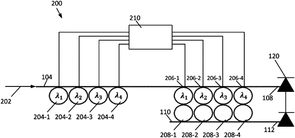
a first waveguide having an input port configured to receive an optical signal comprising M sub-signals each having a respective wavelength, M being an integer greater than or equal to two;
a second waveguide;
M tunable add-drop filters (ADFs) coupled to the first waveguide and to the second waveguide, each of the M tunable ADFs configured to receive a respective tuning signal, each of the M tunable ADFs producing a respective ADF delay of the respective one of the M sub-signals in accordance with a value of the respective tuning signal;
M controllable optical delay elements (ODEs) coupled to the first waveguide, upstream from the M tunable ADFs, each controllable ODE of the M controllable ODEs configured to receive a respective control signal and to impart a respective controllable ODE delay to the respective one of the M sub-signals in accordance with a value of the respective control signal, each of the M sub-signals having associated thereto a respective combined delay equal to a sum of the respective ADF delay and the respective controllable ODE delay, each control signal configured to control each respective controllable ODE delay to produce a substantially same combined delay for each respective sub-signal of the M sub-signals.
|