| CPC G02B 1/11 (2013.01) [B29C 33/424 (2013.01); G02B 1/04 (2013.01); G02F 1/167 (2013.01); G02F 1/1676 (2019.01); G09G 3/344 (2013.01); G09G 3/3446 (2013.01); G02B 1/18 (2015.01); G02B 5/0294 (2013.01); G09G 2300/0421 (2013.01); G09G 2300/0426 (2013.01)] | 4 Claims |
|
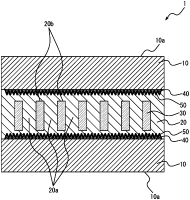
1. An optical device comprising: two substrates provided opposite to each other; a partition wall formed between opposing faces of the two substrates and configured to separate adjacent spaces; and a fluid filled in the spaces separated by the partition wall and containing an electric field control material, wherein
the optical device further comprises, between one of the two substrates and the partition wall, and between the other of the two substrates and the partition wall, respective fine uneven layers having fine uneven shapes and respective conductive layers formed according to shapes of the respective fine uneven layers;
an average distance between unevennesses of the fine uneven layers is 50 to 300 nm and an average height of unevenness of the fine uneven layers is 30 nm or more;
the fine uneven layers are formed on the opposing faces of the two substrates;
the conductive layers cover the fine uneven layers; and
the partition wall is formed between opposing faces of the conductive layers.
|