| CPC G01R 19/18 (2013.01) [G06F 1/04 (2013.01); H03F 3/45475 (2013.01)] | 14 Claims |
|
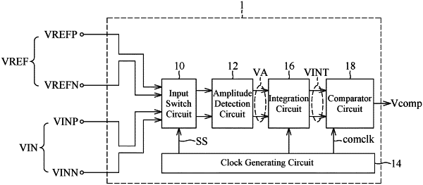
1. A signal detection circuit, comprising:
an input switch circuit configured to receive a reference voltage and an input voltage, and controlled by a switching signal group to selectively output the reference voltage or the input voltage;
an amplitude detection circuit configured to detect an output of the input switch circuit to correspondingly generate an amplitude voltage;
a clock generating circuit configured to generate the switching signal group, wherein the switching signal group is used to control the input switch circuit to alternately enter a first phase and a second phase, and the input switch circuit is controlled to output the reference voltage in the first phase, and output the input voltage in the second phase;
an integration circuit configured to receive the amplitude voltage as an input for performing an accumulation, and generate an integration voltage corresponding to an accumulation result within a predetermined time interval,
wherein the predetermined time interval comprises at least one period that cycles between the first phase and the second phase.
|