| CPC G01J 1/44 (2013.01) [G01J 2001/446 (2013.01)] | 9 Claims |
|
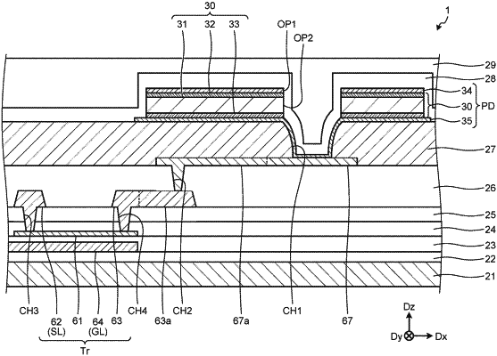
1. A detection device comprising:
a substrate;
a photodiode in which a lower electrode, a semiconductor layer, and an upper electrode are stacked on the substrate in the order as listed;
a transistor provided in the photodiode; and
an insulating layer provided between layers of the transistor and the photodiode, wherein
the insulating layer has a contact hole provided in a central portion of the photodiode in plan view,
the lower electrode of the photodiode is provided on the insulating layer, is provided continuously in an area overlapping the contact hole, and is electrically coupled to the transistor at a bottom of the contact hole, and
a first opening is provided in an area of the upper electrode that overlaps the contact hole.
|