| CPC C09J 183/04 (2013.01) [B32B 7/12 (2013.01); B32B 27/08 (2013.01); C09J 175/04 (2013.01); H05K 5/0017 (2013.01); H05K 9/0024 (2013.01); B32B 2405/00 (2013.01); B32B 2457/08 (2013.01); B32B 2457/208 (2013.01)] | 15 Claims |

|
1. An electronic device comprising:
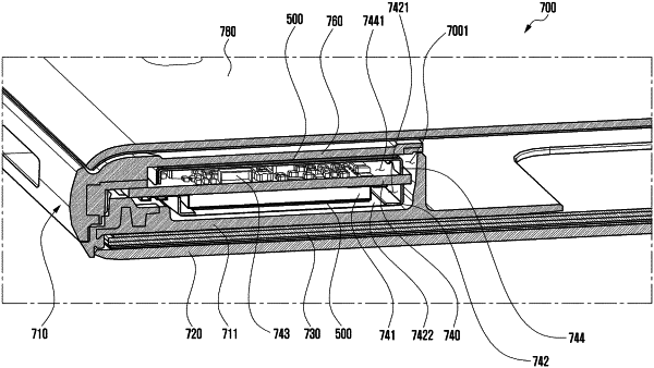
a housing including a first plate, a second plate facing in an opposite direction to the first plate, and a lateral member surrounding a space between the first plate and the second plate;
a printed circuit board (PCB) disposed in the space and having at least one electric element mounted thereon;
a shield can mounted on the PCB and disposed to surround at least in part the at least one electric element; and
an insulating tape member attached to an inner surface of the shield can between the shield can and the electric element, and including:
a first layer containing a first material and formed to have a first thickness;
a second layer laminated on the first layer with an adhesive, containing a second material, and formed to have a second thickness equal to or greater than the first thickness; and
an adhesive layer formed on the second layer and attached to the shield can.
|