| CPC B81C 1/0019 (2013.01) [H10N 30/05 (2023.02); H10N 30/06 (2023.02); H10N 30/093 (2023.02); H10N 30/50 (2023.02); H10N 30/85 (2023.02); H10N 30/87 (2023.02); B82Y 10/00 (2013.01); B82Y 40/00 (2013.01)] | 20 Claims |
|
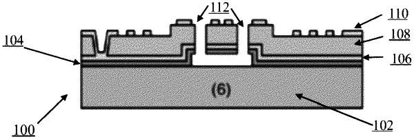
1. A method for fabricating a nano electromechanical system (NEMS), the method comprising:
forming a protective layer above a substrate;
forming a first conductive layer above the protective layer, wherein the first conductive layer forms a first electrode;
forming a piezoelectric layer above the first conductive layer;
forming a second conductive layer above the piezoelectric layer;
patterning the second conductive layer to form a second electrode; and
forming one or more trenches that extends through the first conductive layer, the piezoelectric layer and the second conductive layer, wherein the protective layer, the first and second conductive layers and the piezoelectric layer are optically transparent.
|