| CPC B81B 7/0067 (2013.01) [B81C 1/00317 (2013.01); B81B 2203/0353 (2013.01); B81C 2201/0125 (2013.01); B81C 2201/0132 (2013.01); B81C 2201/0194 (2013.01)] | 9 Claims |

|
1. A manufacturing method of a chip package, comprising:
bonding a carrier onto a metal layer that is on a top surface of a semiconductor substrate by a temporary adhesive layer, wherein the metal layer has plural oxide sections disposed therein;
forming an opening in a bottom surface of the semiconductor substrate such that the semiconductor substrate has a remaining portion between the metal layer and the opening, wherein the semiconductor substrate has a sidewall surrounding the opening;
after forming the opening in the bottom surface of the semiconductor substrate, removing the temporary adhesive layer and the carrier from the metal layer;
after removing the temporary adhesive layer and the carrier from the metal layer, etching the plural oxide sections such that the metal layer forms plural through holes positionally corresponding to where the plural oxide sections were disposed to define a MEMS (Microelectromechanical system) structure; and
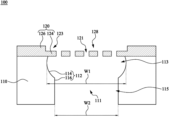
after etching the plural oxide sections, etching the semiconductor substrate to remove the remaining portion of the semiconductor substrate and a portion of the sidewall of the semiconductor substrate, such that an upper portion of the sidewall is a concave surface that faces toward and surrounds the opening, and a lower portion of the sidewall of the semiconductor substrate is a vertical surface that faces toward and surrounds the opening, wherein the semiconductor substrate has no portion in the opening and overlapped with the MEMS structure in a vertical direction.
|