US 11,871,687 B2
Resistive switching element and memory device including the same
Sang Woon Lee, Suwon-si (KR); Tae Joo Park, Ansan-si (KR); Hae Jun Jung, Suwon-si (KR); Sung Min Kim, Incheon (KR); Hye Ju Kim, Suwon-si (KR); and Seong Hwan Kim, Seoul (KR)
Assigned to AJOU UNIVERSITY INDUSTRY-ACADEMIC COOPERATION FOUNDATION, Suwon-si (KR); and INDUSTRY-UNIVERSITY COOPERATION FOUNDATION HANYANG UNIVERSITY ERICA CAMPUS, Ansan-si (KR)
Appl. No. 17/760,967
Filed by AJOU UNIVERSITY INDUSTRY-ACADEMIC COOPERATION FOUNDATION, Suwon-si (KR); and INDUSTRY-UNIVERSITY COOPERATION FOUNDATION HANYANG UNIVERSITY ERICA CAMPUS, Ansan-si (KR)
PCT Filed Sep. 17, 2020, PCT No. PCT/KR2020/012550
§ 371(c)(1), (2) Date Mar. 16, 2022,
PCT Pub. No. WO2021/054737, PCT Pub. Date Mar. 25, 2021.
Claims priority of application No. 10-2019-0113858 (KR), filed on Sep. 17, 2019.
Prior Publication US 2022/0407002 A1, Dec. 22, 2022
Int. Cl. G11C 11/22 (2006.01); H10N 70/00 (2023.01); H10B 63/00 (2023.01)
CPC H10N 70/8833 (2023.02) [H10B 63/80 (2023.02); H10N 70/023 (2023.02); H10N 70/066 (2023.02); H10N 70/841 (2023.02)] 17 Claims
OG exemplary drawing
 
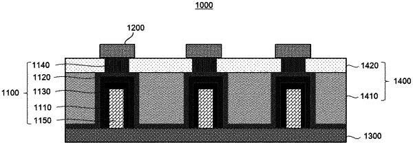
1. A resistive switching element comprising:
a first oxide layer and a second oxide layer stacked one on top of the other such that an interface is present therebetween, wherein the first oxide layer and the second oxide layer are made of different metal oxides;
two-dimensional electron gas (2DEG) present in the interface between the first oxide layer and the second oxide layer and functioning as an inactive electrode; and
an active electrode disposed on the second oxide layer,
wherein when a positive bias is applied to the active electrode, an electric field is generated between the active electrode and the two-dimensional electron gas, such that the second oxide layer is subjected to the electric field, and active metal ions from the active electrode are injected into the second oxide layer.