| CPC H10K 59/40 (2023.02) [G06F 3/0412 (2013.01); G06F 3/0446 (2019.05); H10K 50/844 (2023.02); H10K 59/131 (2023.02)] | 15 Claims |
|
1. A display device comprising:
a display panel including a light emitting element configured to generate light; and
an input detection layer disposed on the display panel and including:
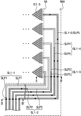
a plurality of sensing electrodes disposed on the display panel and arranged in one direction; and
a plurality of trace lines electrically connected to the plurality of sensing electrodes, respectively,
wherein at least one of the trace lines comprises:
a single layer part including one conductive layer; and
a multilayer part including at least two conductive layers disposed on different layers,
wherein a length of an ith trace line among the trace lines and a length of a jth trace line among the trace lines are different from each other,
wherein each of the ith trace line and the jth trace line comprises the single layer part and the multilayer part, and
wherein a length ratio of the single layer part and the multilayer part of the ith trace line is different from a length ratio of the single layer part and the multilayer part of the jth trace line.
|