| CPC H10K 59/131 (2023.02) [G09G 3/3233 (2013.01); H10K 59/1213 (2023.02); H10K 59/1216 (2023.02); H10K 77/111 (2023.02); G09G 2300/0861 (2013.01); G09G 2310/0251 (2013.01); G09G 2310/0262 (2013.01); G09G 2320/043 (2013.01); H01L 27/124 (2013.01); H01L 27/1255 (2013.01); H01L 28/60 (2013.01); H01L 29/45 (2013.01); H01L 29/4908 (2013.01); H10K 50/80 (2023.02); H10K 2102/311 (2023.02); Y02E 10/549 (2013.01)] | 10 Claims |
|
1. A display device, comprising:
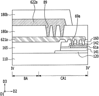
a display panel including a display area for displaying images and a non-display area adjacent to the display area, the non-display area including a bending area and a first contact area between the display area and the bending area;
a first wire transmitting a data signal and including:
a first conductive part disposed in the first contact area,
a second conductive part overlapping the first conductive part and disposed in at to least the first contact area and the bending area, and
a third conductive part overlapping the second conductive part and disposed in at least the first contact area;
a first insulating layer disposed between the first conductive part and the second conductive part; and
a second insulating layer disposed between the second conductive part and the third conductive part,
wherein the second conductive part of the first wire is connected to the first conductive part of the first wire through a first contact hole formed in at least the first insulating layer, and the third conductive part of the first wire is connected to the second conductive part of the first wire through a second contact hole formed in at least the second insulating layer.
|