| CPC H10K 59/131 (2023.02) [H10K 50/844 (2023.02); H10K 59/40 (2023.02)] | 29 Claims |
|
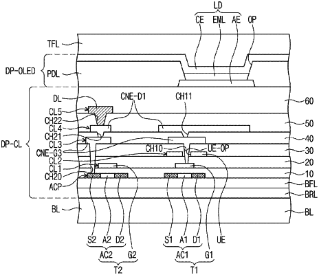
1. A display device, comprising:
a base layer;
a pixel disposed on the base layer;
a signal line electrically connected to the pixel;
a signal pad connected to the signal line; and
a plurality of insulating layers disposed on the base layer,
wherein the signal pad comprises:
a first conductive pattern connected to an end portion of the signal line;
a second conductive pattern connected to the first conductive pattern; and
at least one insulating pattern disposed between the end portion of the signal line and the second conductive pattern in a cross-sectional view and overlapping the second conductive pattern in a plan view,
wherein a first group of insulating layers among the insulating layers is disposed between the end portion of the signal line and the first conductive pattern,
the end portion of the signal line is connected to the first conductive pattern via a first contact hole defined through the first group of insulating layers,
a second group of insulating layers among the insulating layers is disposed between the first conductive pattern and the second conductive pattern, and
the first conductive pattern is connected to the second conductive pattern via a second contact hole defined through the second group of insulating layers.
|