US 11,871,628 B2
Method of manufacturing conductive line for display device including the same
Sukyoung Yang, Hwaseong-si (KR); Sangwoo Sohn, Yongin-si (KR); Dokeun Song, Yongin-si (KR); Dongmin Lee, Anyang-si (KR); Sangwon Shin, Yongin-si (KR); Hyuneok Shin, Gwacheon-si (KR); Kyeong Su Ko, Hwaseong-si (KR); Sang Gab Kim, Seoul (KR); and Joongeol Lee, Jeollabuk-do (KR)
Assigned to Samsung Display Co., Ltd., Yongin-si (KR)
Filed by Samsung Display Co., Ltd., Yongin-Si (KR)
Filed on Feb. 2, 2022, as Appl. No. 17/591,268.
Application 17/591,268 is a division of application No. 16/720,230, filed on Dec. 19, 2019, granted, now 11,271,067.
Claims priority of application No. 10-2019-0009621 (KR), filed on Jan. 25, 2019.
Prior Publication US 2022/0157920 A1, May 19, 2022
Int. Cl. H01L 27/14 (2006.01); H10K 59/131 (2023.01); H10K 59/121 (2023.01)
CPC H10K 59/131 (2023.02) [H10K 59/1213 (2023.02); H10K 59/1216 (2023.02)] 6 Claims
OG exemplary drawing
 
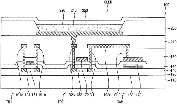
1. A method of manufacturing a display device, comprising:
forming a semiconductor layer on a substrate;
forming a first conductive line on the semiconductor layer; and
forming a second conductive line on the first conductive line, the second conductive line including a first layer including aluminum or an aluminum alloy, a second layer including a refractory metal nitride, and a third layer including a refractory metal,
wherein the third layer of the second conductive line has a multilayer structure including a plurality of stacked sub-layers, and
wherein the forming the second conductive line includes a vacuum break between forming the sub-layers.