| CPC H10K 59/131 (2023.02) [H10K 59/1213 (2023.02); H10K 59/1216 (2023.02); H01L 27/124 (2013.01)] | 11 Claims |
|
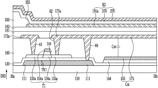
1. A display device comprising:
a substrate;
a first conductive layer including a lower pattern disposed on the substrate;
a first transistor disposed on the substrate and including a first active pattern and a first gate electrode;
a second transistor disposed on the substrate and including a second active pattern and a second gate electrode;
a third transistor disposed on the substrate and including a third active pattern and a third gate electrode; and
a capacitor including a first terminal connected to the first gate electrode, and a second terminal connected to the third transistor, wherein
the lower pattern has a planar area that is greater than a planar area of the first active pattern and overlaps an entirety of the first active pattern, and
the lower pattern includes a portion that does not overlap the first active pattern in a plan view.
|