| CPC H10K 59/124 (2023.02) [G06F 3/0412 (2013.01); G06F 3/0446 (2019.05); G06V 40/1318 (2022.01); H10K 50/858 (2023.02); H10K 59/122 (2023.02); H10K 59/40 (2023.02); H10K 71/00 (2023.02); G06F 2203/04112 (2013.01)] | 22 Claims |
|
1. A display device comprising:
a display panel having a plurality of light emitting areas; and
an input sensor disposed directly on the display panel and including a first conductive layer and a first insulating layer disposed on the first conductive layer,
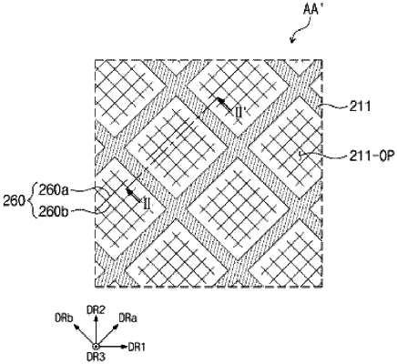
wherein the first insulating layer comprises a plurality of optical patterns comprising a plurality of lens patterns that extend in a direction away from the first conductive layer, the plurality of lens patterns comprising a plurality of first grooves and a plurality of second grooves defined in the first insulating layer,
wherein the plurality of first grooves extend in a first direction and are spaced apart from each other in a second direction intersecting the first direction, and
wherein the plurality of second grooves extend in the second direction and are spaced apart from each other in the first direction.
|