| CPC H10K 59/123 (2023.02) [G09G 3/3233 (2013.01); H10K 59/1213 (2023.02); G09G 2300/0842 (2013.01); G09G 2340/0435 (2013.01); H01L 27/124 (2013.01)] | 19 Claims |
|
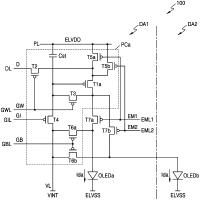
1. A display device comprising:
a first light-emitting element disposed in a first display area;
a second light-emitting element disposed in a second display area different from the first display area;
a first pixel circuit disposed in the first display area, wherein the first pixel circuit outputs a first driving current for driving at least one selected from the first light-emitting element and the second light-emitting element;
a first emission control transistor disposed in the first display area and which connects the first pixel circuit and the first emission control transistor to the first light-emitting element; and
a second emission control transistor disposed in the first display area and which connects the first pixel circuit and the second emission control transistor to the second light-emitting element.
|