| CPC H10K 59/1213 (2023.02) [G09G 3/3266 (2013.01); G09G 3/3291 (2013.01); H01L 27/124 (2013.01); H01L 27/1218 (2013.01); H01L 27/1225 (2013.01); H01L 27/1244 (2013.01); H01L 27/1255 (2013.01); H01L 29/78633 (2013.01); H10K 50/11 (2023.02); H10K 59/122 (2023.02); H10K 59/123 (2023.02); H10K 59/124 (2023.02); H10K 59/126 (2023.02); H10K 59/1216 (2023.02); H10K 59/131 (2023.02); H10K 59/35 (2023.02); H10K 77/111 (2023.02); G09G 2300/0426 (2013.01); G09G 2300/0452 (2013.01); G09G 2330/021 (2013.01); H10K 59/352 (2023.02); H10K 59/353 (2023.02); H10K 2102/341 (2023.02)] | 12 Claims |
|
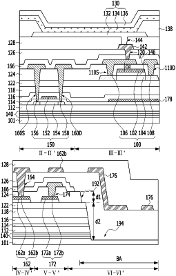
1. A display device comprising:
a flexible substrate comprising an active area and a bending area;
a first thin-film transistor disposed in the active area, the first thin-film transistor comprising a polycrystalline semiconductor layer, a first gate electrode, a first source electrode, and a first drain electrode;
a second thin-film transistor disposed in the active area, the second thin-film transistor comprising an oxide semiconductor layer, a second gate electrode, a second source electrode, and a second drain electrode;
a first planarization layer covering the first thin-film transistor and the second thin-film transistor in the active area, the first planarization layer extending to the bending area;
a connection electrode disposed on the first planarization layer;
a second planarization layer disposed on the first planarization layer including the connection electrode in the active area and the bending area; and
a light emitting element disposed on the first planarization layer in the active area, the light emitting element having an anode and a light emitting stack,
wherein the light emitting stack includes at least one light emitting layer.
|