| CPC H10K 59/1213 (2023.02) [H10K 59/1216 (2023.02); H01L 21/02532 (2013.01); H01L 21/02592 (2013.01); H01L 21/02661 (2013.01); H01L 21/02675 (2013.01); H01L 27/1222 (2013.01); H01L 27/1255 (2013.01); H01L 27/1274 (2013.01); H01L 29/42384 (2013.01); H01L 29/6675 (2013.01); H01L 29/78645 (2013.01); H01L 29/78672 (2013.01); H01L 29/78696 (2013.01); H01L 2029/42388 (2013.01); H10K 59/1201 (2023.02)] | 2 Claims |
|
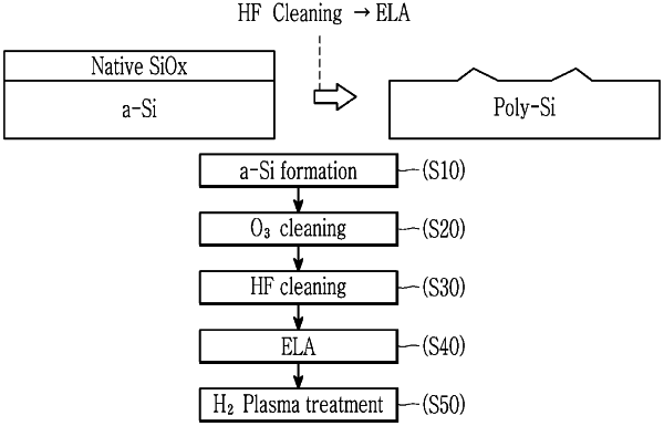
1. A manufacturing method of a light emitting display device, the manufacturing method comprising:
forming amorphous silicon on a substrate;
cleaning the amorphous silicon;
crystallizing the amorphous silicon by irradiating the amorphous silicon with a laser; and
plasma-treating a surface of a crystallized semiconductor with hydrogen;
forming a semiconductor layer by etching the crystallized semiconductor;
forming a first gate insulating film covering the semiconductor layer; and
forming a first gate conductor on the first gate insulating film,
wherein the first gate insulating film is defined by one of a single layer of a silicon oxide film and a double layer of a silicon nitride film and the silicon oxide film,
wherein the first gate insulating film has a thickness value in a range of 800 Å to 1200 Å,
wherein the thickness value of the first gate insulating film is a thickness of the single layer of the silicon oxide film or a converted thickness of the double layer of the silicon nitride film and the silicon oxide film to the thickness of the single layer of the silicon oxide film, and
wherein a length of a channel of a transistor defined by a portion of the semiconductor layer is in a range of 1 μm to 2.5 μm.
|