| CPC H10K 59/1213 (2023.02) [H10K 59/124 (2023.02); H10K 59/126 (2023.02); H10K 59/1216 (2023.02); H01L 27/1225 (2013.01); H01L 27/1251 (2013.01); H01L 27/1255 (2013.01); H01L 29/7869 (2013.01); H01L 29/78633 (2013.01); H01L 29/78675 (2013.01)] | 22 Claims |
|
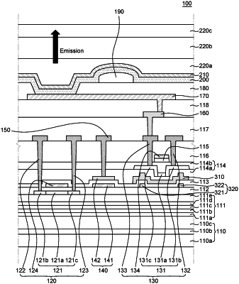
1. An organic light emitting display device, comprising:
a substrate including a first substrate, a second substrate, and an inorganic insulating layer disposed between the first substrate and the second substrate;
a first buffer layer on the substrate;
a first thin film transistor including a first active layer that is formed of a first material and includes a first source region, a first channel region, and a first drain region, a first gate electrode that overlaps the first active layer with a first gate insulating layer interposed therebetween, and a first source electrode and a first drain electrode that are electrically connected to the first active layer;
a second thin film transistor including a second active layer that is formed of a second material and includes a second source region, a second channel region, and a second drain region, a second gate electrode that overlaps the second active layer with a second gate insulating layer interposed therebetween, and a second source electrode and a second drain electrode that are electrically connected to the second active layer;
a storage capacitor including a first capacitor electrode that is disposed on a same layer as the first gate electrode, and a second capacitor electrode that overlaps the first capacitor electrode with a first interlayer insulating layer interposed therebetween;
a light blocking layer overlapping a lower portion of the second active layer and formed on a same layer as the second capacitor electrode; and
a first protrusion pattern and a second protrusion pattern disposed on a same layer as the first gate electrode and overlapping the light blocking layer,
wherein a distance between the first protrusion pattern and the second protrusion pattern is greater than a width of the second channel region of the second active layer.
|