| CPC H10K 59/1213 (2023.02) [H10K 59/1216 (2023.02); H10K 59/131 (2023.02); H10K 59/1201 (2023.02)] | 13 Claims |
|
1. A display device comprising:
a base substrate;
a TFT layer disposed on the base substrate, and including a plurality of pixel circuits arranged; and
a light-emitting element layer disposed on the TFT layer, the light-emitting element layer including a plurality of light-emitting elements arranged in correspondence with the plurality of pixel circuits,
wherein each of the plurality of pixel circuits includes
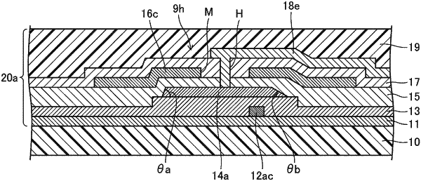
a TFT including a semiconductor layer, a gate insulating film, and a gate electrode, the gate insulating film covering the semiconductor layer, the gate electrode being provided in a form of an island overlapping a part of the semiconductor layer in a plan view on the gate insulating film, and
a capacitor including the gate electrode, a first inorganic insulating film, and a capacitive electrode, the first inorganic insulating film being disposed on the gate electrode, the capacitive electrode overlapping the gate electrode in the plan view on the first inorganic insulating film,
the capacitive electrode extends all around a perimeter of the gate electrode and extends to an outside of the perimeter, and
an angle formed between an upper surface of the base substrate and at least a part of an end surface in a circumferential direction of the gate electrode not overlapping the semiconductor layer in the plan view is greater than an angle formed between the upper surface of the base substrate and an end surface of the gate electrode overlapping the semiconductor layer in the plan view.
|