| CPC H10K 50/805 (2023.02) [H10K 50/15 (2023.02); H10K 50/16 (2023.02); H10K 59/32 (2023.02)] | 20 Claims |
|
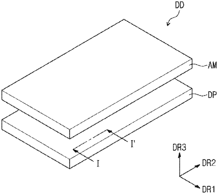
1. A light emitting display device comprising:
a display panel; and
a touch sensing unit on the display panel,
wherein the display panel comprises:
a substrate including a first light emitting region, a second light emitting region, and a non-light emitting region;
a first electrode comprising a first sub-electrode on the first light emitting region and a second sub-electrode on the second light emitting region;
a first light emitting unit on the first electrode;
a charge generation unit comprising an n-type charge generation layer on the first light emitting unit and a p-type charge generation layer on the n-type charge generation layer;
a second light emitting unit on the charge generation unit; and
a second electrode on the second light emitting unit,
wherein the first light emitting unit comprises a first light emitting layer on the first sub-electrode, and a second light emitting layer on the second sub-electrode,
wherein the second light emitting unit comprises a third light emitting layer on the first light emitting layer, and a fourth light emitting layer on the second light emitting layer,
wherein one of the n-type charge generation layer and the p-type charge generation layer comprises a first sub charge generation layer on the first light emitting region and a second sub charge generation layer on the second light emitting region.
|