| CPC H01L 51/5203 (2013.01) [G09G 3/32 (2013.01); G09G 3/3233 (2013.01); H01L 27/1108 (2013.01); H01L 27/3262 (2013.01); H01L 51/0096 (2013.01); G09G 2300/0426 (2013.01); G09G 2300/0814 (2013.01); G09G 2300/0842 (2013.01); G09G 2300/0861 (2013.01); G09G 2300/0866 (2013.01); G09G 2310/0245 (2013.01); G09G 2310/0262 (2013.01); H01L 27/3265 (2013.01); H01L 51/0023 (2013.01); H01L 51/5296 (2013.01); H01L 2227/323 (2013.01)] | 19 Claims |
|
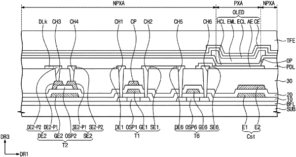
1. A display device comprising:
a base substrate;
a first transistor above the base substrate and comprising a first semiconductor pattern below first, second, and third insulation layers and a first gate between the first insulation layer and the second insulation layer;
a second transistor above the base substrate and comprising a second gate between the first insulation layer and the second insulation layer, a second semiconductor pattern between the second insulation layer and the third insulation layer, and a third gate above the first, second, and third insulation layers and electrically connected to the second gate;
a third transistor above the base substrate and comprising a third semiconductor pattern below the first, second, and third insulation layers and a fourth gate between the first insulation layer and the second insulation layer;
a first conductive pattern on the first gate and overlapping the first gate;
at least one second conductive pattern on the third insulation layer; and
a light emitting diode above the third insulation layer,
wherein the third insulation layer is disposed between the first conductive pattern and the third gate,
the first semiconductor pattern comprises a polysilicon semiconductor and the second semiconductor pattern comprises an oxide semiconductor,
a first through hole is defined in the first, second, and third insulation layers to correspond to the first semiconductor pattern,
a second through hole is defined in the third insulation layer to correspond to the second semiconductor pattern, and
each of the first through hole and the second through hole is filled with a corresponding conductive pattern of the at least one second conductive pattern.
|