| CPC H10K 30/865 (2023.02) [H10K 50/805 (2023.02); H10K 50/841 (2023.02); H10K 59/12 (2023.02); H10K 71/00 (2023.02)] | 5 Claims |
|
1. A method of manufacturing an organic light-emitting display device, the method comprising:
simultaneously forming a pixel electrode and an auxiliary electrode on a substrate;
forming a first insulating film between the pixel electrode and the auxiliary electrode to cover an end of the pixel electrode and an end of the auxiliary electrode;
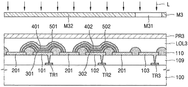
sequentially forming a lift-off layer and a photoresist on the pixel electrode, the auxiliary electrode, and the first insulating film;
forming an opening exposing an upper surface of the pixel electrode by patterning the lift-off layer and the photoresist;
sequentially forming an intermediate layer comprising an emission layer, an opposite electrode, and a passivation layer in the opening and on the photoresist, wherein the opposite electrode in the opening contacts the auxiliary electrode while covering the intermediate layer; and
removing the lift-off layer and the photoresist.
|