| CPC H10B 51/20 (2023.02) [H01L 29/516 (2013.01); H01L 29/517 (2013.01); H10B 43/20 (2023.02); H10B 43/30 (2023.02); H10B 51/30 (2023.02)] | 9 Claims |
|
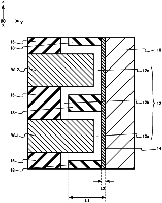
1. A semiconductor memory device comprising:
a semiconductor layer extending in a first direction;
a first gate electrode layer;
a second gate electrode layer provided apart from the first gate electrode layer in the first direction; and
a gate insulating layer containing oxygen (O) and at least one metal element of hafnium (Hf) or zirconium (Zr), the gate insulating layer including a first region, a second region, and a third region, the first region provided between the first gate electrode layer and the semiconductor layer, the second region provided between the first gate electrode layer and the second gate electrode layer, and the third region provided between the second gate electrode layer and the semiconductor layer, the first region including a crystal of an orthorhombic crystal system or a trigonal crystal system as a main constituent substance, and a distance between the second region and the semiconductor layer being larger than a distance between the first region and the semiconductor layer,
wherein the first gate electrode layer includes a first portion and a second portion closer to the semiconductor layer than the first portion, and a length of the second portion in the first direction is shorter than a length of the first portion in the first direction.
|