| CPC H10B 43/50 (2023.02) [H01L 21/76224 (2013.01); H01L 21/76805 (2013.01); H01L 23/535 (2013.01); H10B 43/10 (2023.02); H10B 43/27 (2023.02); H10B 43/40 (2023.02); H01L 21/31111 (2013.01); H01L 21/31116 (2013.01)] | 20 Claims |

|
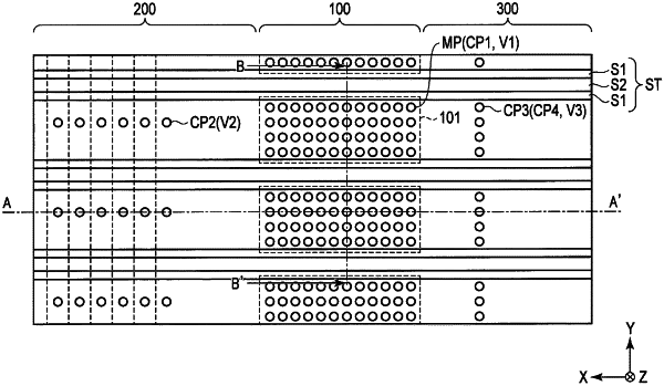
1. A semiconductor memory device comprising:
a stacked body provided above a substrate, in which conductive layers are isolated from each other and stacked along a first direction crossing a surface of the substrate;
a source layer provided between the substrate and the stacked body;
memory pillars passing through the stacked body along the first direction, one ends of the memory pillars being coupled to the source layer respectively;
first contacts coupled to the other ends of the memory pillars respectively;
first vias of which one ends are coupled to the first contacts and the other ends are coupled to bit lines respectively;
a first insulation film provided above the stacked body, the first insulation film being located higher than upper surfaces of the memory pillars in the first direction;
isolation portions passing through the stacked body and the first insulation film along the first direction, extending in a second direction crossing the first direction and isolating the stacked body in a third direction crossing the first direction and the second direction;
a first member including silicon and nitrogen provided above the first insulation film, the first member being located between the one ends and the other ends of the first vias in the first direction;
through contacts provided in holes formed through the first insulation film and the stacked body along the first direction within a region between two isolation portions adjacent in the third direction of the isolation portions; and
a lower interconnect provided between the substrate and the source layer, wherein
a first through contact of the through contacts is provided in one hole of the holes, the first through contact having a side wall insulation layer provided on a side wall of the one hole and any through contact other than the first through contact being not provided in the one hole, and
the first through contact is electrically connected to the lower interconnect while being electrically insulated from the source layer.
|