US 11,871,576 B2
Semiconductor memory device including integrated control circuit and solid-state drive controller
Yoshiaki Fukuzumi, Yokkaichi (JP); Hideaki Aochi, Yokkaichi (JP); Mie Matsuo, Yokkaichi (JP); Kenichiro Yoshii, Bunkyo (JP); Koichiro Shindo, Yokohama (JP); Kazushige Kawasaki, Kawasaki (JP); and Tomoya Sanuki, Yokkaichi (JP)
Assigned to Kioxia Corporation, Tokyo (JP)
Filed by Kioxia Corporation, Tokyo (JP)
Filed on Dec. 7, 2020, as Appl. No. 17/113,285.
Application 17/113,285 is a continuation of application No. 16/409,637, filed on May 10, 2019, granted, now 10,892,269.
Application 16/409,637 is a continuation in part of application No. 16/121,123, filed on Sep. 4, 2018, abandoned.
Application 16/121,123 is a continuation in part of application No. 15/388,318, filed on Dec. 22, 2016, granted, now 10,090,315, issued on Oct. 2, 2018.
Application 15/388,318 is a continuation of application No. 14/806,034, filed on Jul. 22, 2015, granted, now 9,558,945, issued on Jan. 31, 2017.
Claims priority of application No. 2014-186684 (JP), filed on Sep. 12, 2014.
Prior Publication US 2021/0118898 A1, Apr. 22, 2021
Int. Cl. H10B 43/40 (2023.01); H01L 25/065 (2023.01); H01L 25/18 (2023.01); H10B 43/27 (2023.01); H10B 43/30 (2023.01); H10B 43/50 (2023.01); H01L 21/18 (2006.01); H01L 21/768 (2006.01); H01L 23/00 (2006.01)
CPC H10B 43/40 (2023.02) [H01L 21/185 (2013.01); H01L 21/76898 (2013.01); H01L 24/80 (2013.01); H01L 25/0657 (2013.01); H01L 25/18 (2013.01); H10B 43/27 (2023.02); H10B 43/30 (2023.02); H10B 43/50 (2023.02); H01L 2224/08145 (2013.01)] 15 Claims
OG exemplary drawing
 
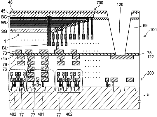
1. A semiconductor memory device comprising:
a semiconductor substrate;
a control circuit provided on the semiconductor substrate;
a solid state drive controller provided on the semiconductor substrate;
a first interconnection layer provided above the control circuit and the solid state drive controller;
a second interconnection layer provided above the first interconnection layer and including a plurality of bit lines; and
a three-dimensionally disposed plurality of memory cells above the plurality of bit lines and electrically connected to the control circuit through the first interconnection layer and the second interconnection layer, wherein
the control circuit is electrically connected to the solid state drive controller through the first interconnection layer,
a plurality of transistors consisting of the solid state drive controller are located on at least two areas of the semiconductor substrate, and
the control circuit includes at least one transistor disposed on an area between two areas among the at least two areas of the semiconductor substrate.