| CPC H10B 43/35 (2023.02) [H10B 43/10 (2023.02); H10B 43/27 (2023.02)] | 11 Claims |
|
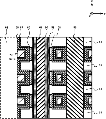
1. A semiconductor memory device comprising:
a first interlayer insulating layer and a second interlayer insulating layer arranged in a first direction;
a gate electrode layer provided between the first interlayer insulating layer and the second interlayer insulating layer;
a semiconductor layer extending in the first direction and facing the gate electrode layer in a second direction intersecting the first direction;
a first insulating layer provided between the gate electrode layer and the semiconductor layer;
a charge storage layer provided between the gate electrode layer and the first insulating layer and containing a metal element;
a second insulating layer provided between the gate electrode layer and the charge storage layer;
a first region provided between the charge storage layer and the first insulating layer and containing manganese (Mn), silicon (Si), and oxygen (O),
a second region provided between the charge storage layer and the first interlayer insulating layer, and containing manganese (Mn), silicon (Si), and oxygen (O); and
a third region provided between the charge storage layer and the second interlayer insulating layer, and containing manganese (Mn), silicon (Si), and oxygen (O).
|