| CPC H10B 12/30 (2023.02) [H01L 21/02603 (2013.01); H01L 21/28518 (2013.01); H01L 21/30604 (2013.01); H01L 29/0673 (2013.01); H01L 29/42392 (2013.01); H01L 29/66742 (2013.01); H01L 29/78696 (2013.01); H10B 12/01 (2023.02); H10B 12/05 (2023.02); H10B 12/482 (2023.02); H10B 12/50 (2023.02)] | 20 Claims |
|
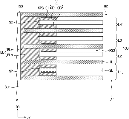
14. A method for manufacturing a semiconductor memory device, the method comprising:
forming a stack structure including a plurality of semiconductor layers vertically stacked on a substrate;
forming a first hole and a second hole, the first hole and the second hole penetrating the stack structure;
partially etching the plurality of semiconductor layers exposed by the first and second holes to divide each of the plurality of semiconductor layers into a pair of semiconductor patterns;
forming a vertical insulator filling the first and second holes;
forming a gate electrode on the pair of semiconductor patterns;
forming a bit line on a side of the stack structure, the bit line extending vertically;
replacing a portion of each of the semiconductor patterns with a first electrode, the first electrode extending horizontally;
forming a second electrode on the first electrode; and
forming a dielectric layer between the first electrode and the second electrode.
|