| CPC H05K 1/115 (2013.01) [H05K 1/0298 (2013.01); H05K 1/111 (2013.01); H05K 1/116 (2013.01); H05K 1/165 (2013.01)] | 20 Claims |
|
1. A wiring substrate, comprising:
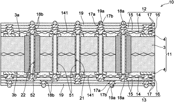
an insulating layer having a through hole;
a first conductor layer formed on a first surface of the insulating layer;
a second conductor layer formed on a second surface of the insulating layer on an opposite side with respect to the first surface of the insulating layer;
a magnetic body penetrating through the insulating layer along a thickness direction of the insulating layer such that the through hole is formed through the magnetic body; and
an inductor comprising an interlayer connection conductor formed in the through hole and penetrating through the magnetic body such that the interlayer connection conductor is connecting the first and second conductor layers, and a resin body formed in the through hole of the insulating layer such that a volume occupancy rate of the resin body is in a range of 30% to 55% in the through hole,
wherein the interlayer connection conductor of the inductor is formed such that the interlayer connection conductor has a length in a range of 1000 μm to 2000 μm in the thickness direction of the insulating layer and that a volume occupancy rate of the interlayer connection conductor is in a range of 45% to 70% in the through hole.
|