| CPC H05K 1/0298 (2013.01) [H01L 21/4857 (2013.01); H01L 23/5383 (2013.01); H01L 23/5385 (2013.01); H05K 1/115 (2013.01); H05K 3/245 (2013.01); H01L 23/467 (2013.01); H05K 2201/09618 (2013.01)] | 18 Claims |
|
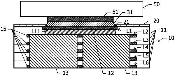
1. A multilayer wiring substrate including conductive layers and insulating layers alternately stacked on each other, each of the conductive layers having a conductive pattern, a semiconductor device being mounted on a top surface of the multilayer wiring substrate, the multilayer wiring substrate comprising:
a protective film that covers the conductive pattern of a first conductive layer of the conductive layers, the first conductive layer being a topmost layer of the conductive layers, at least one cavity being formed in the protective film to expose part of the conductive pattern of the first conductive layer, the at least one cavity being elongated in one direction;
at least one first via-conductor that extends downward from the conductive pattern of the first conductive layer at least until the conductive pattern of a second conductive layer, the second conductive layer being a second layer; and
a plurality of second via-conductors that extend downward from the conductive pattern of the second conductive layer or a third conductive layer of the conductive layers, the third conductive layer being a third layer, at least until the conductive pattern of a conductive layer of the conductive layers one below the second conductive layer or the third conductive layer, wherein
the at least one first via-conductor is between the plurality of second via-conductors and the semiconductor device, and
when one of a longitudinal direction of the at least one cavity and a direction perpendicular to the longitudinal direction and parallel with the top surface of the multilayer wiring substrate is defined as a first direction,
as viewed from above, at least one of
one or some of the at least one first via-conductor, and
one or some of the plurality of second via-conductors
overlaps the at least one cavity, and extends from inside the at least one cavity toward both sides in the first direction so as to at least partially protrude from the at least one cavity.
|