| CPC H04N 23/52 (2023.01) [H04N 23/54 (2023.01)] | 7 Claims |
|
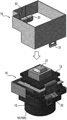
1. An electronic device comprising:
a first substrate and a second substrate with respective main surfaces, and on each of which an electronic component is mounted, the first substrate and the second substrate positioned in a stacking direction with the respective main surfaces facing each other;
a first metal plate including
a flat portion that is interposed between the first substrate and the second substrate, and that directly or indirectly abuts the electronic component mounted on the first substrate and the electronic component mounted on the second substrate, and a first shield portion that covers a portion of a side surface of the first substrate; and
a second metal plate including
a second shield portion that surrounds a circumference of the second substrate and covers another portion of the side surface of the first substrate that is not covered by the first shield portion, wherein the second shield portion does not cover the portion of the side surface of the first substrate that is covered by the first shield portion,
wherein the first metal plate and the second metal plate abut each other directly or indirectly.
|