| CPC H03K 17/284 (2013.01) [H02M 1/08 (2013.01); H02M 7/53871 (2013.01); H02P 27/08 (2013.01); H03K 2217/0063 (2013.01); H03K 2217/0072 (2013.01)] | 14 Claims |
|
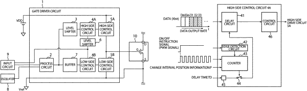
1. Electronic circuitry comprising:
a control circuit configured to control a drive circuit for a semiconductor device; and
a delay circuit configured to receive a first signal instructing the drive circuit to drive the semiconductor device with first driving force and output the first signal to the control circuit,
wherein the delay circuit is configured to receive a second signal at an interval of a first time or “n” times of the first time after the first signal is received, “n” being an integer greater than or equal to 2, and the second signal instructing the drive circuit to drive the semiconductor device with second driving force, and
the delay circuit is configured to delay outputting of the second signal for a delay time shorter than the first time, and output the second signal to the control circuit after the first signal is outputted and further after the first time or “n” times of the first time and the delay time elapses.
|