| CPC H03K 17/0822 (2013.01) [G05F 3/262 (2013.01); H01L 29/2003 (2013.01); H03K 17/6871 (2013.01)] | 20 Claims |
|
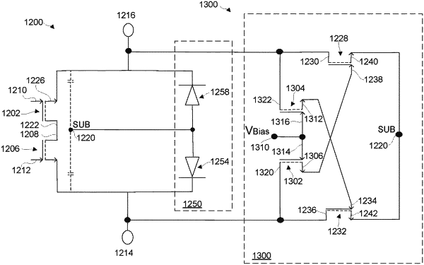
1. An electronic device, comprising:
a gallium nitride (GaN) substrate comprising a GaN-based top layer attached to a silicon-based bottom layer;
a bidirectional transistor switch formed on the GaN-based top layer and including a first source node, a second source node and a common drain node;
a first transistor formed on the GaN-based top layer and including a first source terminal, a first drain terminal and a first gate terminal, the first source terminal connected to the silicon-based bottom layer, the first drain terminal connected to the first source node and the first gate terminal coupled to the second source node;
a second transistor formed on the GaN-based top layer and including a second source terminal, a second drain terminal and a second gate terminal, the second source terminal connected to the silicon-based bottom layer, the second drain terminal connected to the second source node and the second gate terminal coupled to the first source node;
a third transistor formed on the GaN-based top layer and including a third drain, a third source and a third gate, the third gate connected to a voltage source, the third drain connected to the first source node and the third source connected to the second gate terminal; and
a fourth transistor formed on the GaN-based top layer and including a fourth drain, a fourth source and a fourth gate, the fourth gate connected to the voltage source, the fourth drain connected to the second source node, and the fourth source connected to the first gate terminal.
|