| CPC H03K 17/063 (2013.01) [H03K 17/08122 (2013.01); H03K 17/687 (2013.01); H03K 2217/0081 (2013.01)] | 9 Claims |
|
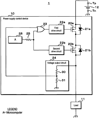
1. A power supply control device for controlling a power supply by switching on or off both a first semiconductor switch and a second semiconductor switch that are arranged on a current path and each have two ends between which a parasitic diode is connected, comprising:
a processing unit configured to perform processing that gives an instruction to switch the first semiconductor switch and the second semiconductor switch on or off; and
a switching circuit configured to switch the first semiconductor switch on, if current flows through the current path even though the processing unit has given an instruction to switch the first semiconductor switch and the second semiconductor switch off,
wherein the cathodes of the parasitic diodes of the first semiconductor switch and the second semiconductor switch are located respectively downstream and upstream of the respective anode on the current path.
|