| CPC H03K 17/04206 (2013.01) | 5 Claims |
|
1. A capacitor-insulated semiconductor relay that maintains insulation between input and output in the semiconductor relay using capacitors, the semiconductor relay comprising:
a pair of input terminals;
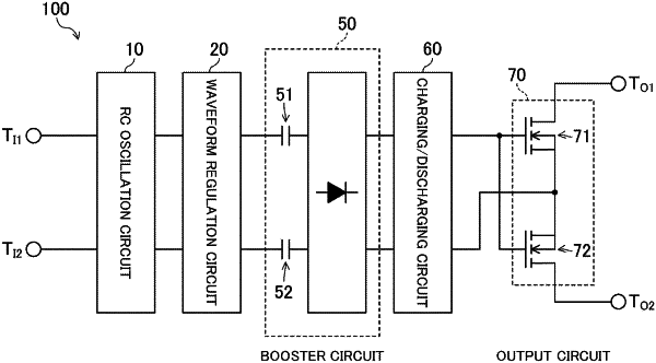
an RC oscillation circuit connected to the pair of input terminals and configured to oscillate in response to an input signal to generate a first signal and a second signal that are inverse in phase to each other;
a waveform regulation circuit configured to receive the first signal and the second signal, and increase rise and fall times of the first signal, and rise and fall times of the second signal;
a booster circuit configured to receive signals outputted from the waveform regulation circuit to generate a predetermined voltage;
a charging/discharging circuit connected to the booster circuit;
an output circuit connected to the charging/discharging circuit; and
a pair of output terminals connected to the output circuit,
wherein the booster circuit being a charge pump circuit having a first high dielectric strength capacitor and a second high dielectric strength capacitor connected in parallel to each other,
the RC oscillation circuit including a plurality of stages of inverters connected in series, and a feedback resistor and a feedback capacitor connected in parallel to the plurality of stages of inverters,
the waveform regulation circuit having a first circuit configured to increase the rise and fall times of the first signal, and a second circuit configured to increase the rise and fall times of the second signal,
the first high dielectric strength capacitor being configured to receive input of a signal outputted from the first circuit, the second high dielectric strength capacitor being configured to receive input of a signal outputted from the second circuit,
the first circuit and the second circuit each include a plurality of stages of CMOS inverters connected in series,
a drain of a p-channel MOSFET in a second-to-last-stage CMOS inverter among the plurality of stages of CMOS inverters and a drain of an n-channel MOSFET in the second-to-last-stage CMOS inverter are electrically connected to each other via a resistive element, and
a gate of a p-channel MOSFET in a last-stage CMOS inverter among the plurality of stages of CMOS inverters is electrically connected to one end of the resistive element, and a gate of an n-channel MOSFET in the last-stage CMOS inverter is electrically connected to an opposite end of the resistive element,
the p-channel MOSFET in the last-stage CMOS inverter has a first capacitor connected in parallel to the gate of the p-channel MOSFET, and the n-channel MOSFET in the last-stage CMOS inverter has a second capacitor connected in parallel to the gate of the n-channel MOSFET, and
the output circuit being configured to be driven based on the voltage generated by the booster circuit.
|