| CPC H03G 3/3036 (2013.01) [H03F 3/19 (2013.01); H03F 3/21 (2013.01); H03M 1/124 (2013.01); H03F 2200/453 (2013.01)] | 30 Claims |
|
1. An apparatus comprising:
a pipeline analog-to-digital converter comprising:
at least two stages; and
at least one amplification circuit coupled between the at least two stages, the at least one amplification circuit comprising:
an amplifier having a gain that is based on a bias voltage and an amplification control signal; and
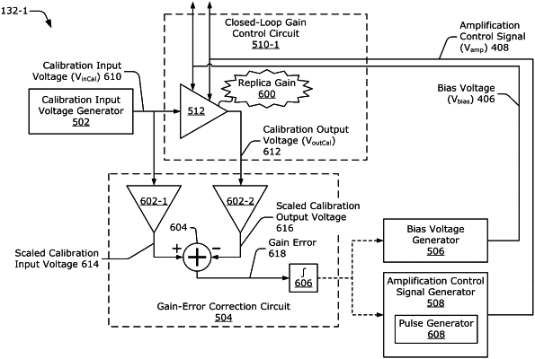
a gain-stabilization circuit coupled to the amplifier, the gain-stabilization circuit comprising:
a replica amplifier corresponding to the amplifier, the replica amplifier configured to have a replica gain that is based on the bias voltage and the amplification control signal,
the gain-stabilization circuit configured to adjust at least one of the bias voltage or the amplification control signal based on a difference between an input voltage and an output voltage of the replica amplifier.
|