| CPC H03B 5/06 (2013.01) [H01L 27/092 (2013.01); H01L 27/1207 (2013.01); H01L 27/1225 (2013.01); H01L 27/1255 (2013.01); H01L 29/7869 (2013.01); H03K 3/014 (2013.01); H03K 3/0315 (2013.01)] | 18 Claims |
|
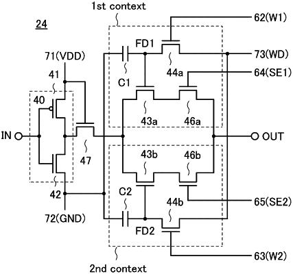
1. A semiconductor device comprising:
first to ninth transistors; and
first and second capacitors,
wherein the first transistor is a p-channel transistor,
wherein the second to ninth transistors are n-channel transistors,
wherein a gate of the first transistor is electrically connected to a gate of the second transistor,
wherein one of a source and a drain of the first transistor is electrically connected to one of a source and a drain of the second transistor and one of a source and a drain of the fifth transistor,
wherein the other of the source and the drain of the first transistor is electrically connected to a gate of the fifth transistor,
wherein a gate of the third transistor is electrically connected to one of a source and a drain of the fourth transistor and a first electrode of the first capacitor,
wherein a second electrode of the first capacitor is electrically connected to the other of the source and the drain of the second transistor,
wherein one of a source and a drain of the third transistor is electrically connected to the other of the source and the drain of the fifth transistor,
wherein the other of the source and the drain of the third transistor is electrically connected to one of a source and a drain of the sixth transistor,
wherein the other of the source and the drain of the fifth transistor is directly connected to one of a source and a drain of the seventh transistor,
wherein the other of the source and the drain of the seventh transistor is electrically connected to one of a source and a drain of the ninth transistor,
wherein a gate of the seventh transistor is electrically connected to one of a source and a drain of the eighth transistor and a first electrode of the second capacitor,
wherein a second electrode of the second capacitor is electrically connected to the other of the source and the drain of the second transistor, and
wherein the other of the source and the drain of the ninth transistor is electrically connected to the other of the source and the drain of the sixth transistor.
|