| CPC H02N 2/028 (2013.01) [G02B 26/0833 (2013.01); G02B 26/101 (2013.01); H02N 2/22 (2013.01); H10N 30/06 (2023.02); H10N 30/87 (2023.02)] | 13 Claims |
|
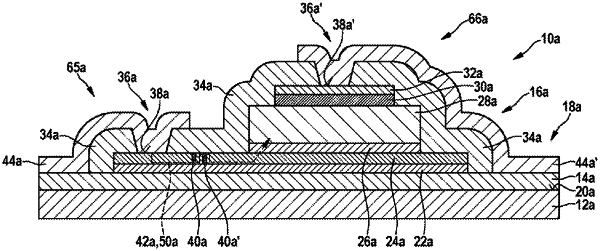
1. A microelectronics device, comprising:
at least one bearer substrate; and
at least one layered piezo stack situated on the bearer substrate, the piezo stack having at least one piezo element and at least one electrode; and
at least one contact opening situated on the at least one electrode;
wherein:
the microelectronics device has at least one diffusion blocking element that is situated on the at least one electrode at least partly at a distance from the piezo element, and/or
the at least one contact opening forms a contact surface that is at most as large as one one-thousandth of a surface of the at least one piezo element, and/or
a length of an electrical path from the at least one contact opening to the at least one piezo element corresponds to at least twice a circumference of the at least one contact opening.
|