| CPC H02H 9/046 (2013.01) [H02H 1/0007 (2013.01)] | 13 Claims |
|
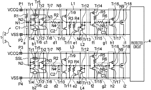
1. A semiconductor device comprising a first protection circuit and a second protection circuit for protecting a protected circuit,
the first protection circuit comprising
a timer circuit connected between a first pad connected to a power supply potential and a second pad connected to a reference potential and configured to output a control signal for controlling operation periods of the first protection circuit and the second protection circuit,
a voltage detection circuit connected between the first pad and the second pad on an output side of the timer circuit and configured to operate based on the control signal and output a discharge instruction signal when a voltage between the first pad and the second pad exceeds a first threshold voltage, and
a discharge element connected between the first pad and the second pad on an output side of the voltage detection circuit and configured to discharge from the first pad to the second pad in response to the discharge instruction signal, and
the second protection circuit comprising a discharge circuit connected between a third pad connected to the power supply potential and a fourth pad connected to the reference potential on the output side of the timer circuit and configured to discharge from the third pad to the fourth pad when a voltage between the third pad and the fourth pad exceeds a second threshold voltage.
|