| CPC H01S 5/0208 (2013.01) [H01S 5/04256 (2019.08); H01S 5/04257 (2019.08); H01S 5/12 (2013.01); H01S 5/2275 (2013.01); H01S 5/0283 (2013.01); H01S 5/2224 (2013.01)] | 13 Claims |
|
1. A semiconductor laser device comprising:
a substrate; and
a semiconductor layer provided on the substrate and including a first conductivity type contact layer,
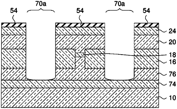
wherein a mesa is provided in the semiconductor layer and includes a resonator and a second conductivity type contact layer,
grooves are provided on opposing sides of the mesa,
a top surface of the first conductivity type contact layer and a side face of the mesa including at least one end face of the resonator construct an L shape,
the top surface of the first conductivity type contact layer constructs a bottom surface of the L shape,
for each of the grooves, a side face of the groove includes a first slope near the bottom surface of the groove and a first side face above the first slope, the first side face being substantially perpendicular to the bottom surface of the groove,
a side face of the L shape includes a second slope near the bottom surface of the L shape and a second side face above the second slope, the second side face being substantially perpendicular to the bottom surface of the L shape,
a first electrode is connected to the first conductivity type contact layer and the first electrode is positioned directly on the bottom surface of at least one of the grooves,
a second electrode is connected to the second conductivity type contact layer,
the first conductivity type contact layer forms the bottom surfaces of the grooves,
the first side face and the second side face being formed by dry etching until a portion of the first conductivity type contact layer is exposed, and
the first slope and the second slope being formed by wet etching after the dry etching.
|