| CPC H01S 5/0071 (2013.01) [G02B 6/002 (2013.01); G02B 6/0031 (2013.01); G02B 6/0068 (2013.01); H01S 5/4093 (2013.01)] | 9 Claims |
|
1. An illumination device comprising:
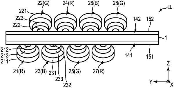
a light guide including a first plane, a second plane opposed to the first plane and substantially parallel to the first plane, a side plane, a first tilted plane located between the side plane and the first plane and tilted to the first plane, and a second tilted plane located between the side plane and the second plane and tilted to the second plane, an angle formed between the side plane and the first tilted plane and an angle formed between the side plane and the second tilted plane being acute angles;
a first semiconductor laser element including a first base and a first light emitting part; and
a second semiconductor laser element including a second base and a second light emitting part,
wherein
the first base and the second base are non-parallel to each other,
the first light emitting part is opposed to a first intersection part of the side plane and the first tilted plane,
the second light emitting part is opposed to a second intersection part of the side plane and the second tilted plane,
a thickness of the light guide in an area where the first tilted plane and the second tilted plane are opposed to each other, is increased toward the side plane, and
a thickness of the light guide in an area where the first plane and the second plane are opposed to each other, is less than a thickness of the light guide in the side plane.
|