| CPC H01L 33/145 (2013.01) [H01L 27/156 (2013.01); H01L 33/005 (2013.01); H01L 33/04 (2013.01); H01L 33/56 (2013.01)] | 22 Claims |
|
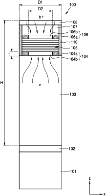
1. A nanorod light-emitting device comprising:
a first semiconductor layer doped with a first conductivity type;
a light-emitting layer on the first semiconductor layer;
a second semiconductor layer disposed on the light-emitting layer and doped with a second conductivity type that is electrically opposite to the first conductivity type;
at least one conductive layer disposed between a central portion of a lower surface of the light-emitting layer and the first semiconductor layer, or between a central portion of an upper surface of the light-emitting layer and the second semiconductor layer;
at least one current blocking layer that surrounds a side surface of the at least one conductive layer; and
an insulating film that surrounds a side surface of the second semiconductor layer, a side surface of the light-emitting layer, and a side surface of the at least one current blocking layer,
wherein a diameter of the first semiconductor layer of the nanorod light-emitting device and an outer diameter of the insulating film of the nanorod light-emitting device are both in a range of 0.05 μm to 2 μm, and
wherein an upper surface of the first semiconductor layer contacts a lower surface of the insulating film.
|