| CPC H01L 29/78696 (2013.01) [G02F 1/1368 (2013.01); G02F 1/13439 (2013.01); G06F 1/1643 (2013.01); G06F 1/1652 (2013.01); G06F 3/0412 (2013.01); H01L 27/1225 (2013.01); H01L 29/045 (2013.01); H01L 29/24 (2013.01); H01L 29/66969 (2013.01); H01L 29/786 (2013.01); H01L 29/7869 (2013.01); H01L 29/78648 (2013.01); H10K 59/00 (2023.02); G02B 27/017 (2013.01); G02F 1/1345 (2013.01); G02F 1/13338 (2013.01); G02F 1/13454 (2013.01); G02F 1/134381 (2021.01); G02F 2202/10 (2013.01); G06F 3/0445 (2019.05); G06F 2203/04103 (2013.01); H10K 59/1213 (2023.02); H10K 59/40 (2023.02)] | 18 Claims |
|
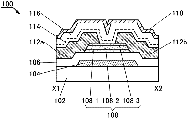
1. A semiconductor device comprising:
a substrate;
a first conductive layer over the substrate;
a first insulating layer over the first conductive layer;
an oxide semiconductor layer over the first insulating layer;
a second conductive layer over the oxide semiconductor layer;
a third conductive layer over the oxide semiconductor layer; and
a second insulating layer over the second conductive layer and the third conductive layer,
wherein the oxide semiconductor layer comprises a first oxide semiconductor film and a second oxide semiconductor film,
wherein the second oxide semiconductor film comprises a region having lower crystallinity than the first oxide semiconductor film,
wherein the second oxide semiconductor film is a composite oxide semiconductor,
wherein the composite oxide semiconductor comprises:
a first region comprising InaMbZncOd; and
a second region comprising InxZnyOz,
wherein the a, b, c, d, x, y, and z each represent a given number,
wherein the M represents Al, Ga, Y, or Sn, and
wherein a concentration of indium in the second region is higher than a concentration of indium in the first region.
|