| CPC H01L 29/7869 (2013.01) [G02F 1/1368 (2013.01); G02F 1/133514 (2013.01); H01L 27/1225 (2013.01); H01L 27/1248 (2013.01); G02F 1/136209 (2013.01); G02F 1/136222 (2021.01); H01L 29/78618 (2013.01)] | 14 Claims |
|
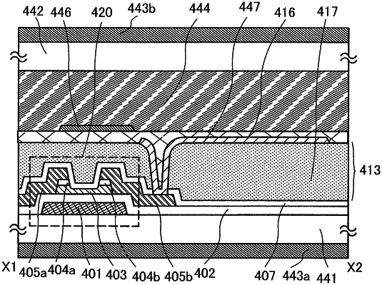
1. A liquid crystal display device comprising:
a gate wiring layer;
a transistor comprising an oxide semiconductor layer overlapping with the gate wiring layer;
a first insulating film over each of the transistor and the gate wiring layer;
a light-transmitting chromatic color resin layer above the first insulating film;
a first electrode layer above the light-transmitting chromatic color resin layer and electrically connected to the transistor;
a second insulating film above the first electrode layer;
a second electrode layer above the second insulating film;
a liquid crystal layer above each of the first electrode layer and the second electrode layer; and
a wiring layer below the first insulating film and electrically connected to the second electrode layer,
wherein the light-transmitting chromatic color resin layer overlaps with the transistor,
wherein in a plan view the wiring layer extends a direction generally parallel to the gate wiring layer,
wherein in the plan view the second electrode layer comprises a first portion generally parallel to the gate wiring layer and a second portion having a comb-shape,
wherein the oxide semiconductor layer includes a crystal having a diameter of 1 nm to 10 nm, and
wherein the crystal contains indium, gallium, and zinc.
|