| CPC H01L 29/7827 (2013.01) [H01L 27/0629 (2013.01); H01L 29/4236 (2013.01); H01L 29/66666 (2013.01)] | 6 Claims |
|
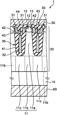
1. A semiconductor device, comprising:
an upper electrode;
a lower electrode;
a n-type substrate positioned between the upper electrode and the lower electrode;
a buried electrode part positioned between the substrate and the upper electrode, the buried electrode part including a gate electrode; and
a silicon layer positioned between the substrate and the upper electrode,
the silicon layer including
a mesa part next to the buried electrode part, and
a n-type drift layer being in direct contact with the n-type substrate, the drift layer including a first region positioned between the mesa part and the substrate, and a second region positioned between the buried electrode part and the substrate,
the first region and the second region being continuous in a direction in which the buried electrode part and the mesa part are next to each other,
an energy level density of the first region being greater than an energy level density of the second region, and a peak of an energy level density of the drift layer being located in the first region.
|