| CPC H01L 29/7397 (2013.01) [H01L 21/76816 (2013.01); H01L 29/0696 (2013.01); H01L 29/0804 (2013.01); H01L 29/0821 (2013.01); H01L 29/0834 (2013.01); H01L 29/1004 (2013.01); H01L 29/401 (2013.01); H01L 29/417 (2013.01); H01L 29/42368 (2013.01); H01L 29/42376 (2013.01); H01L 29/456 (2013.01); H01L 29/66348 (2013.01); H01L 29/7396 (2013.01); H01L 29/8613 (2013.01)] | 9 Claims |
|
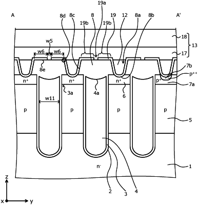
1. A semiconductor device, comprising:
a trench provided at a predetermined depth from a first main surface of a semiconductor substrate;
a gate electrode provided via a gate insulating film in the trench;
an insulating film provided on the first main surface of the semiconductor substrate and covering the gate electrode;
a contact hole penetrating the insulating film in a depth direction and reaching the semiconductor substrate;
a first groove provided in a semiconductor part of the semiconductor substrate exposed in the contact hole,
a metal film provided from a side wall of the contact hole and along an inner wall of the first groove, the metal film adhering to the semiconductor part;
a second groove provided in a part of the metal film and penetrating the metal film in a direction of thickness and reaching a surface of the insulating film facing toward the first electrode;
a metal layer embedded in the metal film in the contact hole; and
a first electrode provided at a surface of the metal layer and the insulating film, wherein
a surface of the gate electrode is positioned within the trench.
|