| CPC H01L 29/7371 (2013.01) [H01L 23/4824 (2013.01); H01L 23/535 (2013.01); H01L 24/13 (2013.01); H01L 27/0823 (2013.01); H01L 29/0692 (2013.01); H01L 29/40 (2013.01); H01L 29/41708 (2013.01); H03F 3/19 (2013.01); H01L 24/05 (2013.01); H01L 24/16 (2013.01); H01L 2224/0401 (2013.01); H01L 2224/1302 (2013.01); H01L 2224/13013 (2013.01); H01L 2224/16227 (2013.01); H01L 2924/13051 (2013.01); H03F 2200/408 (2013.01); H03F 2200/451 (2013.01)] | 17 Claims |
|
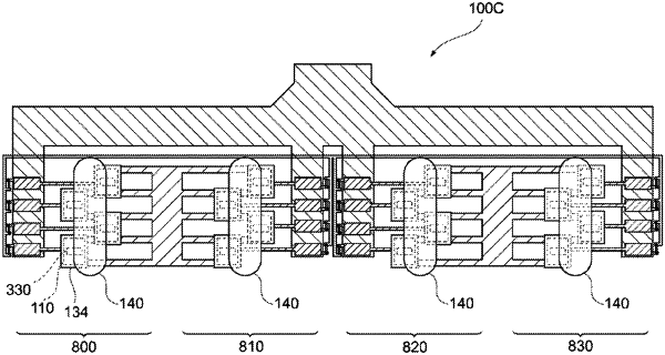
1. A semiconductor device comprising:
a heterojunction bipolar transistor including a plurality of unit transistors;
a plurality of capacitors, each capacitor being electrically connected between an RF input wire and a base wire for each unit transistor of the plurality of unit transistors; and
an emitter wire electrically connected to emitters of the plurality of unit transistors,
wherein
the plurality of unit transistors are arranged in a first direction,
the emitter wire is disposed above the emitters of the plurality of unit transistors,
the plurality of unit transistors include at least one first unit transistor and at least one second unit transistor,
the emitter of the first unit transistor being disposed in the first direction,
the emitter of the second unit transistor being disposed in the first direction,
the emitter of the first unit transistor and the emitter of the second unit transistor are provided in a staggered arrangement,
each of the capacitors is not covered by the emitter wire,
a length of the base wire connected to the first unit transistor is different from a length of the base wire connected to the second unit transistor, and
a distance of the capacitor for the first unit transistor to the emitter of the first unit transistor is less than a distance of the capacitor for the second unit transistor to the emitter of the second unit transistor.
|